


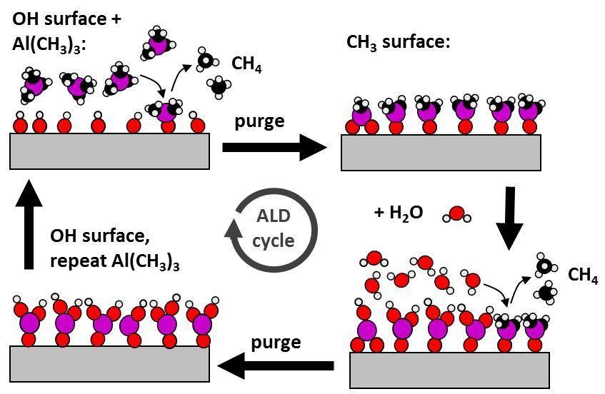
Atomic layer deposition – ALD technology
Experimental research work with the atomic layer deposition (ALD) technology application for thin film deposition in the Optical Coatings Laboratory was started in 2017. This technology ensures a high-quality, stable, repetitive thin layer structure on surfaces, which can range from 1-2 m to nano-structures such as nano-filaments, nano-tubes. In recent years, there has been a growing interest in the use of ALD for optical coatings manufacture, where up to now physical vapor deposition technologies (thermal evaporation, ion beam and magnetron sputtering) have dominated. The application of ALD technology is especially important for optical coatings manufacture on complicated structures (low-radius, multi-prism prisms, gratings, etc.), small dimensions (1-3 mm and less) optical components.
Characterization of optical elements using laser radiation
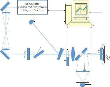
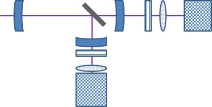
With the rapid development in laser technology, the requirements for optical elements are increasing. They should not only have complex and precise spectral properties, but should also be of high laser radiation resistance. In 2016, an automated laser stand was created for testing such properties of optical coatings in the laboratory.
The main researches carried out are as follows:
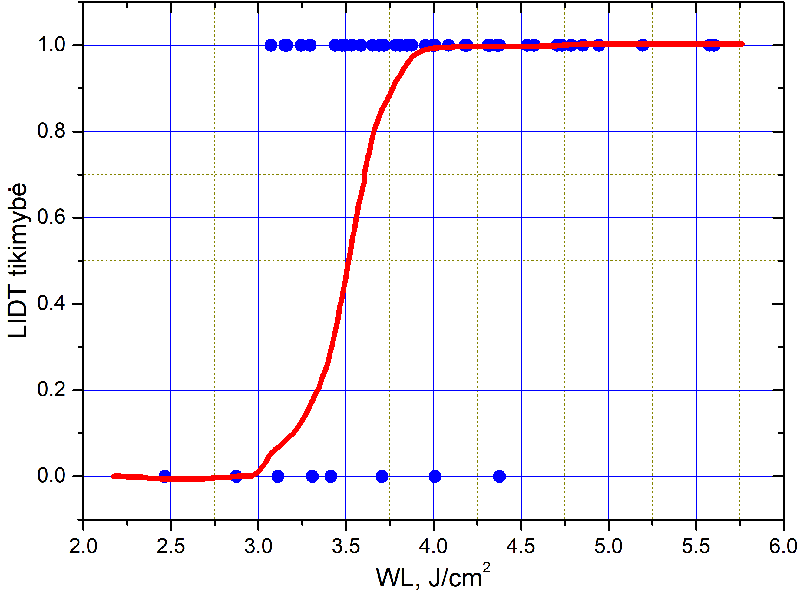
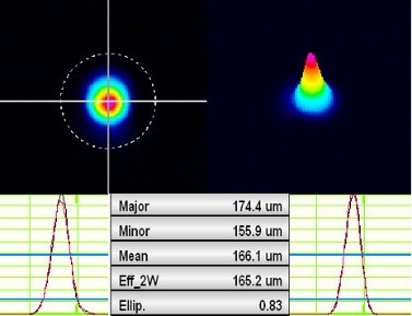
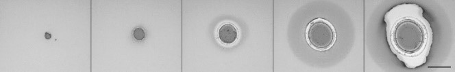
- Resistance of optical elements to laser radiation (according to the ISO-11254 standard and slightly modified using microfocusing tests). Influence of defects on optical resistance. Assessment of the quality of the coatings according to the morphology of the damage.
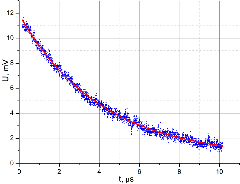
- Evaluation of mirror reflection coefficients using CRD methodology for different angles of incidence and polarization.
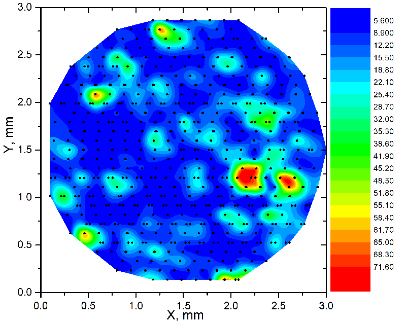
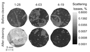
- Determination of the distribution of scattering of optical elements (“mapping”) at a fixed angle.
Coatings with intended dispersion for controlling ultrashort pulse duration
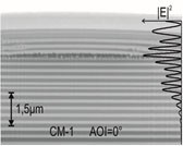
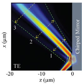
In the process of ultrashort pulse generation, it is important to effectively compensate the positive dispersion accumulated along the propagation distance of the pulse. For this purpose, chirp mirrors are used to create anomalous dispersion in such optical coatings due to different penetration depths and resonant effects.
The main tasks addressed in this topic are:
- Increase optical resistance of chirped mirrors to ultrashort laser pulses.
- Mirrors with an extremely high Group Delay Dispersion (GDD up to 10 000 fs2).
- Wide spectral range chirped mirrors pairs with a reduced GDD oscillations.


Optical coatings with exclusive parameters
Extreme properties of optical and laser systems require exceptionally high parameters of optical elements. The Optical Coatings Laboratory is developing research in the following groups of parameters:
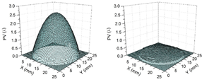
- Coatings with compensated internal stresses and high surface flatness.
- Extremely high laser radiation resistance coatings (LIDT ~ 100 J/cm2 @ 1064 nm).
- Coatings with very low scattering and absorption losses (<1-10 ppm @ 532-1064 nm).
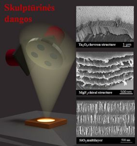
Glancing Angle Deposition technology (GLAD)
Deposition using GLAD technology allows to change and control the angle between the vapor flow and the substrate surface. In this way, multilayer coatings can provide different porosity and structure of individual layers. This technology is very important for the formation of dielectric mirrors and anti-reflection coatings using only SiO2 material, since such coatings exhibit extremely high laser radiation resistance compared to standard coatings. Multilayer structures, namely waveplates and polarizers for zero angle of incidence, can also be formed using GLAD technology.
In the Optical Coatings Laboratory, sculptural coatings are formed and investigated from other materials (SiO2, LaF3, Al2O3, etc.). The formation of such layers on nanostructured surfaces are obtained and the unique properties of such coatings also under investigation.
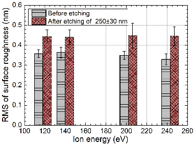
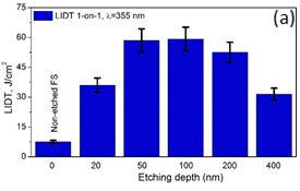
Investigation of optical substrates surface preparation for high power laser optics.
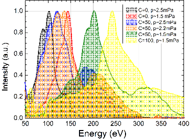
Polished optical substrates have subsurface damage layer, which absorbs laser radiation and drastically decreases optical resistance. Research activities are performed using oxygen and argon plasma in order to remove this subsurface layer. Main tasks are:
- Investigation of plasma properties and etching depth impact on optical substrates surface roughness and their optical resistance.
- Application of etched optical substrates for making anti-reflective, polarizing, spectrum separating coatings and investigation of their optical resistance.

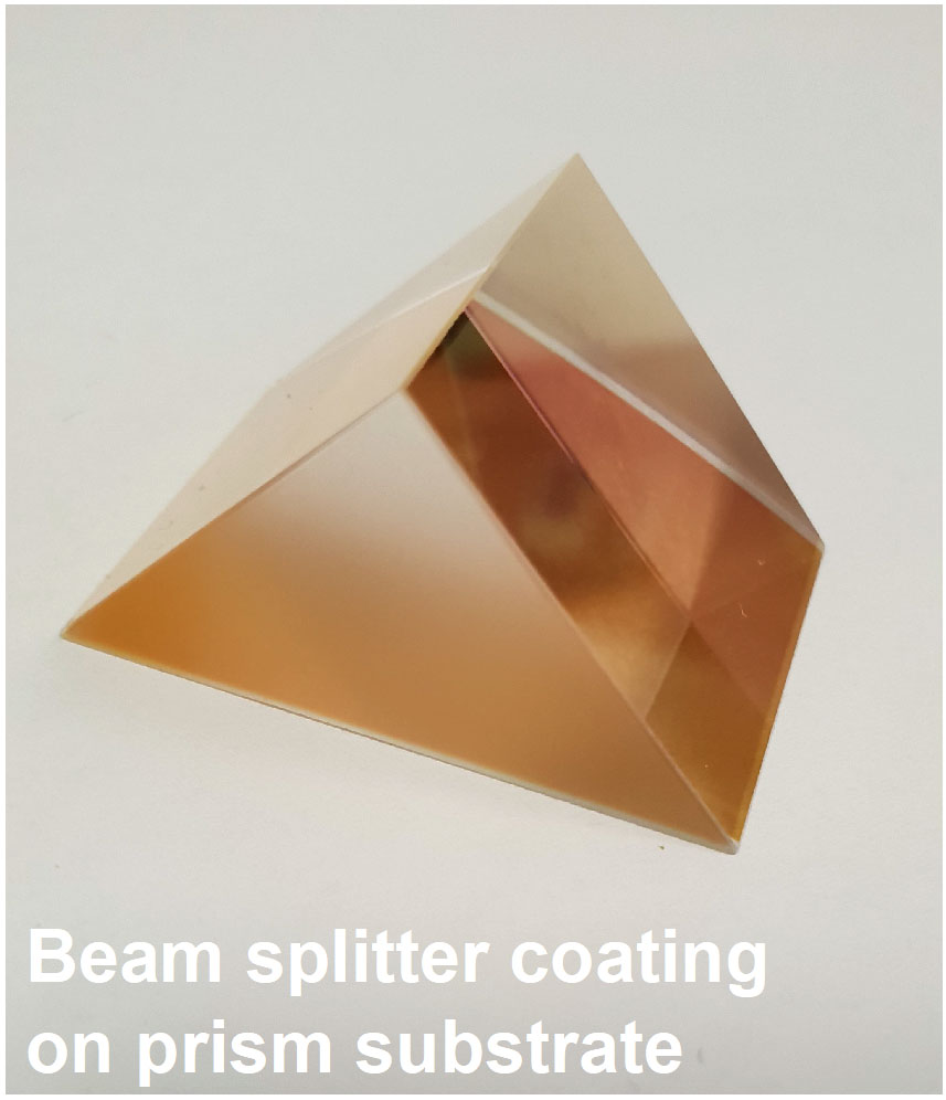
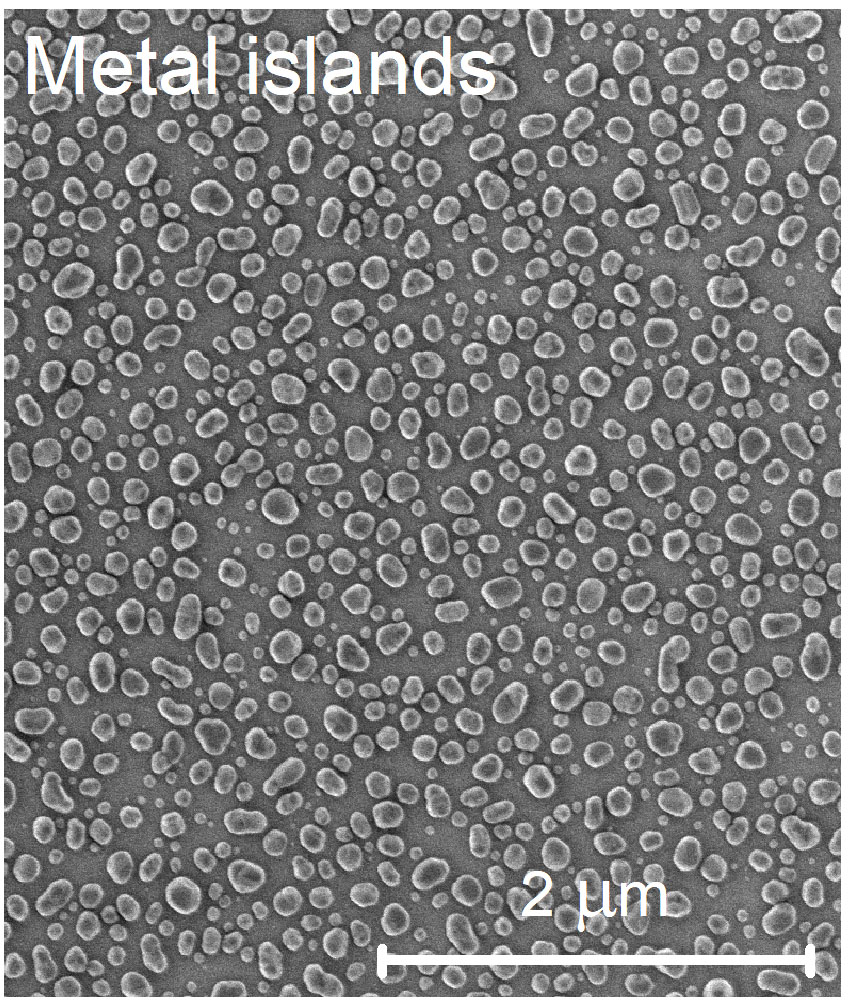
Formation and investigation of optical coatings with ultra-thin metal layers.
Optical components are typically fabricated by coating of optical substrates by dielectric layers. The combination of dielectric coatings with metallic (Al, Au, Ag, Cu, etc.) layers let us to create optical components with unique properties. In a case of ultra-thin noble metal films, they might be non-continuous or continuous. The growth and structure of film greatly depends on the substrate preparation conditions and the technological parameters. The films might have nonlinear optical phenomenas, for example, localized surface plasmons.
By precisely controlling of ultra-thin metal films manufacturing parameters both continuous and islands might be produced. The properties of such films are widely used in the manufacture of broadband or wide-angle beam spliters, absorbers, solar cells and sensors.