


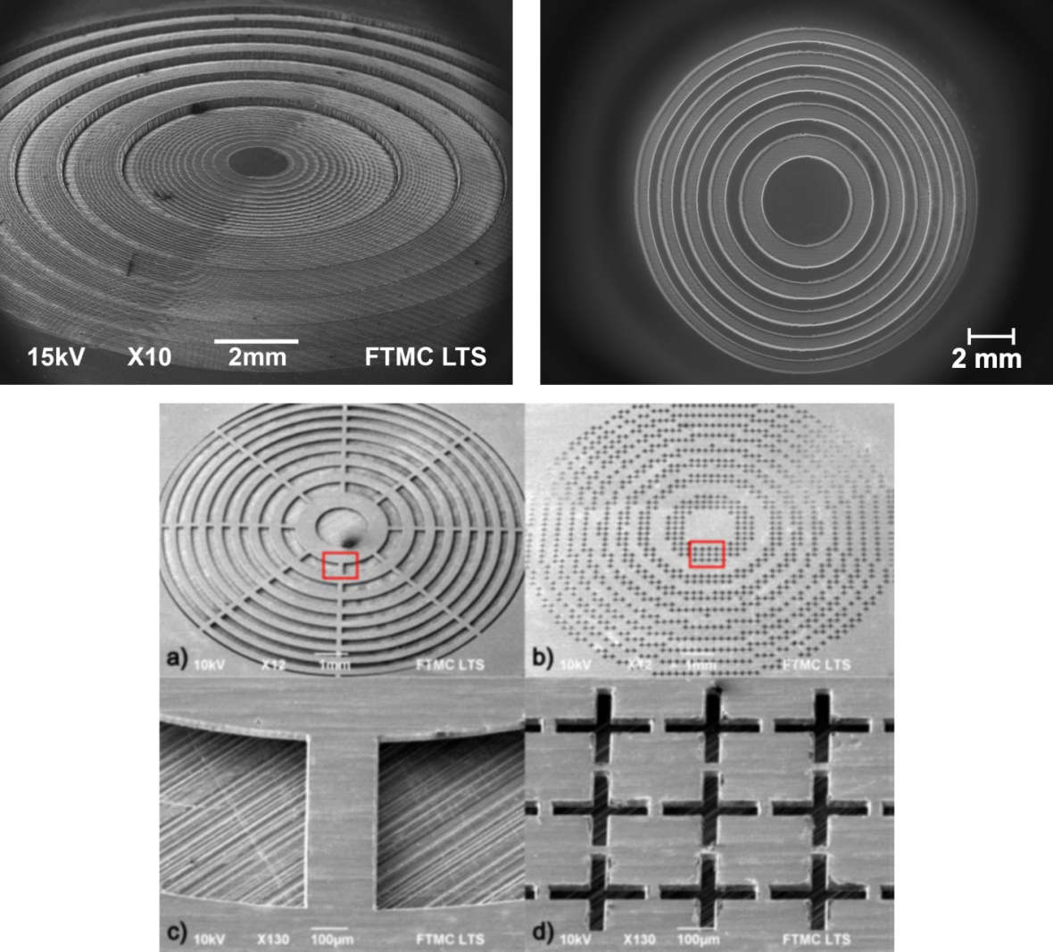
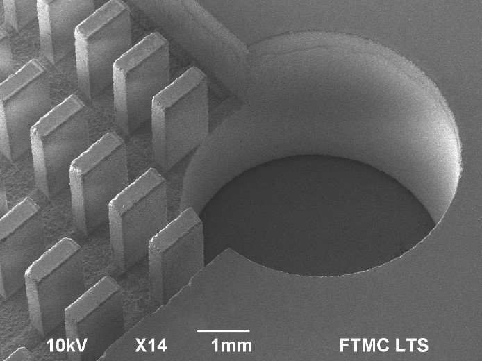
Deep 3D laser engraving technology
The FTMC has developed a fast, deep 3D laser engraving technology. The technology can be applied for various materials processing. During the preparation stage, the 3D object drawing is divided to individual layers. Afterwards, layer by layer material ablation is introduced. The use of picosecond laser pulses for processing ensures high processing quality and speed. Compared to nanosecond lasers, the short pulse – matter interaction time significantly reduces the thermal effects. The laser induced heat diffusion is limited at such pulse durations. Therefore, melt formation and oxidation of the surface are significantly reduced. Also burr formation is much lower compared to nanosecond laser processing. In the case of copper, 6 mm3/min ablation rate is achieved.
Materials: metals, semiconductors, ceramics, glass, polymers.
Ablation precision: 50 μm.
Ablation rate: 6 mm3/min (copper)
More information:
https://www.sciencedirect.com/science/article/abs/pii/S0143816618309102


Laser ablation technology for the fabrication of THz optical components
Laser ablation technology for the fabrication of terahertz optical components was created in cooperation with the FTMC Terahertz photonics laboratory.
This technology is used for the manufacture of diffractive silicon and metal lenses (zone plates) and metal resonance band pass filters.
Optical components for the 0.1 – 5 THz frequency range can be manufactured. Aperture of the optical element ranges from 10 to 25 mm.
More information:
https://www.osapublishing.org/ol/abstract.cfm?uri=ol-42-10-1875
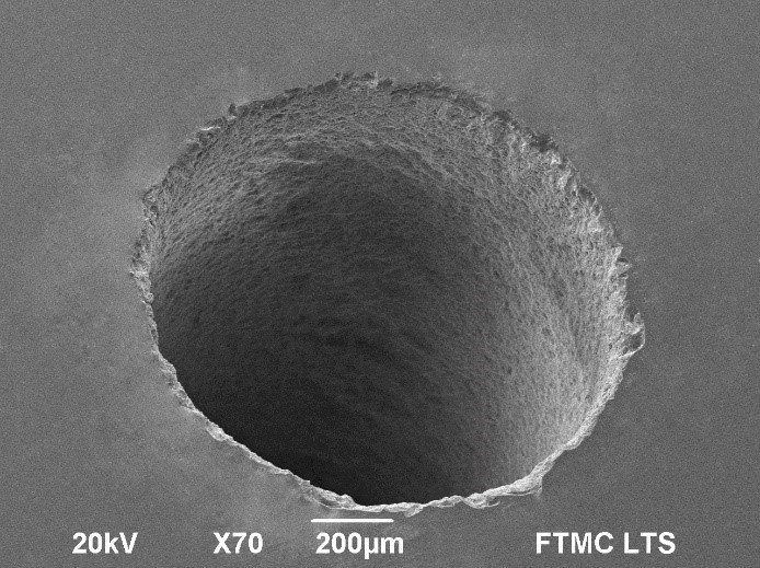
Precision processing of glass by laser
Glass is an important engineering material for a number of different applications. Laser machining of transparent materials, such as flat glass, is fast growing market, driven by new developments in displays, optoelectronics and medical device technology. Conventional glass processing techniques such as diamond drilling and dicing, water-jet drilling, sand blasting or ultrasonic processing are still commonly used in mass production, although limitations of these techniques in flexibility, processing speed and quality requires search for novel technological solutions. Laser based techniques such as rear side glass processing can offer high quality and throughput, which can be used for glass drilling, cutting and milling applications. Typical kerf widths with such technique can be extremely reduced compared to mechanical diamond tool processing, therefore laser milled feature sizes can be reduced to 150 µm. Furthermore, laser cuts are taper – less, therefore extremely high aspect ratio features can be fabricated. Glass surface chipping during processing is another important issue. However, laser based processing can maintain high throughput with highest processing quality keeping surface chipping bellow 100 µm.
Materials: soda lime glass (SLG), fused silica, BK7 glass, borosilicate glass;
Quality: Surface chipping <100 µm, sidewall roughness <2 µm;
Cutting throughput: 0.6 m/min (1 mm SLG glass), 0.12 m/min (5 mm SLG glass);
Via drilling Ø 0.2-1 mm: 1 s/via (1 mm SLG), 5 s/via (5 mm SLG);
Material removal rate: >90 mm3/min.
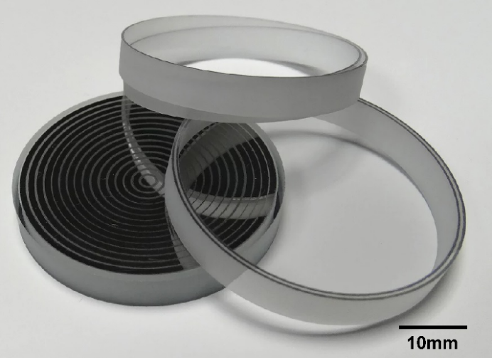
Efficient dicing of sapphire wafers
The evidence of multi-photon absorption enhancement by combined dual-wavelength double-pulse laser irradiation in transparent sapphire was demonstrated experimentally and explained theoretically for the first time in FTMC. The new innovative effect allowed utilisation of laser energy up to four times more efficiently for internal modification initiation in sapphire. This method opens new opportunities for manufacturers of the GaN-based light-emitting diodes by fast and precise separation of sapphire substrates. More information about invention can be found www.nature.com/articles/s41598-017-05548-x

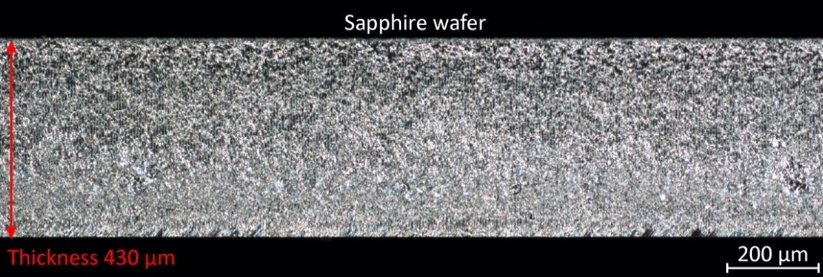
Efficient dicing of sapphire wafers using burst laser
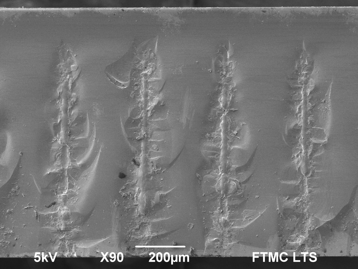
Laser dicing of glass with Bessel beam
Conventional processing tools of glass are facing serious challenges in terms of processing speed and quality. While nowadays most of the laser processing is dedicated for thin, especially chemically strengthened glass, there is still a need for a suitable processing technique for thick glasses. One of the most material-efficient and energy-efficient glass cutting techniques is to locally weaken the material along the cutting path by generating cracks or material modifications and then separate sheets by applying thermal or mechanical load. Bessel beams, have very appealing properties for processing of transparent materials, such as the long non-diffractive propagation length and self-reconstruction. We demonstrate the possibility to cut glasses up to 5 mm thickness by applying Bessel beam induced modifications. The cutting process can offer high cutting efficiency, were 1 mm thick glass sheet can be cut with speed of 240 mm/s. Finally, we demonstrated the possibility to control the transverse crack orientation. The control of the crack propagation direction gives a possibility to form a uniform cutting path in such way, that cracks are always aligned parallel to the scanning direction. This enables us to optimize dicing speed and quality.

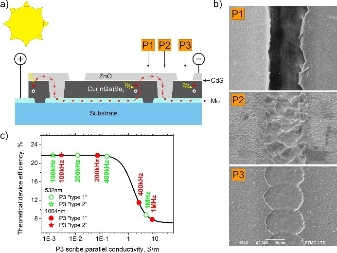
Laser patterning for CIGS devises
Cu-chalcopyrite based solar cells, such as Cu(In,Ga)Se2 (generally called CIGS) have been established as the most efficient thin-film technology in converting sunlight into electricity. In order to maintain high efficiency over the large area, laser scribing is needed to divide large scale device into smaller cells interconnected in series. Usually, three laser scribing processes called P1, P2 and P3 are used for the module processing. Layer selectivity, low thermal damage and high throughput are the main requirements for the industrial scribing processes. To realize these goals, FTMC is carrying out CIGS processing research with modern high power ultra-short pulsed lasers. Most of the work is concentrated on the P2 and P3 high speed scribing.
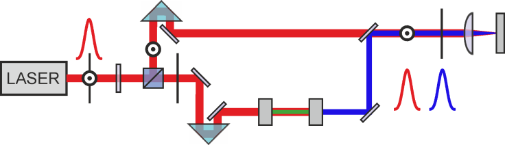
Nano-structuring by combined laser irradiation
Laser induced periodic surface structures have found many applications during the last decade: control of surface wetting; friction reduction; colouring the surfaces; light absorption enhancement.
FTMC has developed the flexible method of nano-surface-structuring by using temporally and spectrally combined laser irradiation. The periodical nano-structures with controllable period varying from 200 nm to 600 nm were successfully fabricated on the stainless steel surface. More information pubs.rsc.org/en/content/articlelanding/2015/ra/c5ra14210e#!divAbstract
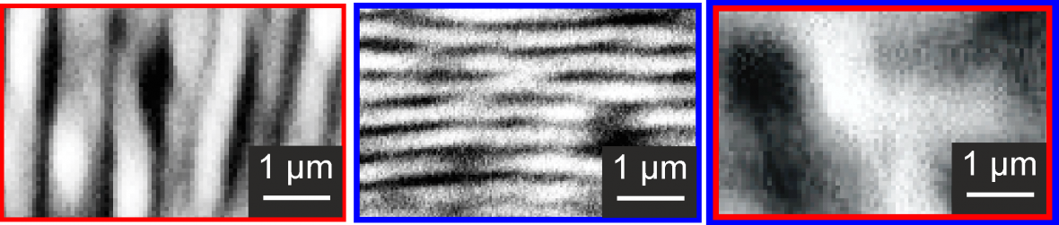
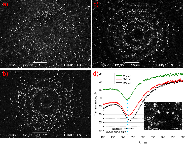
Structuring of Surfaces with Gold Nanoparticles by Using Bessel-Like Beams
The structuring of surfaces with gold nanoparticles by using Bessel-like beam array is demonstrated. The experimental results show that the fabricated microring structures containing gold nanoparticles have a surface plasmon resonance in the spectral range of 520-540 nm, which can be tuned by selecting the laser treatment parameters. Fabricated microring structures exhibit a lower light transmittance comparing with the randomly distributed gold nanoparticles for wavelengths 500-570 nm due to the growth in the size of nanoparticles. The demonstrated method enables an easy fabrication of microring structures having tunable plasmonic properties.
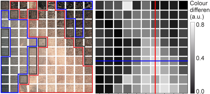
Quality evaluation method of copper deposition
FTMC developed a novel colour-difference measurement method for the quality evaluation of copper deposited. Laser-induced selective activation was performed onto the surface of polymer and copper deposited by using the electroless copper plating procedure. The sheet resistance was found to decrease by the power law with the colour-difference of the sample images after after and before copper deposition. A new colorimetric method is an easy tool for evaluation of the metal plating quality. For more information visit www.nature.com/articles/srep22963